
Step 1 - Ordering of PCB and electronic components
| Material | Data from Github |
| Tools | Computer with internet access |
| Needed Skills |
Basic PC knowledge |
| Time | circa 90 minutes |
The first step to build up the hardware is ordering a PCB. Most of the Libre Solar components are too complex to be produced at home, so you will have to order the PCBs. This step-by-step guide will show how to obtain all necessary data for the fab house. We will use the Libre Solar MPPT charge controller as an example, but the steps are the same for all other projects.
Download of hardware files
Clone or download
It is not recommended to use the Clone or download button on GitHub, as it does not automatically download the library submodule. If you still want to use it or you don’t have the command-line git available, you should also click the library folder on GitHub and download it manually to your already cloned project. Otherwise your schematics will not work and you will get lots of warnings.
Command line
Use your favourite command line tool and type
git clone --recursive https://github.com/LibreSolar/MPPT-Charger_20A
in your desired directory.
After that, open the KiCad project file in KiCad.
Bill of Materials
The Bill of Materials (BOM) lists all the parts of the PCB and is one of the most important documents for the manufacturing process.
In KiCad, the part properties like manufacturer, part number, etc. are defined inside the schematic editor. The Libre Solar schematics contain the following fields:
- Reference
- Value
- Footprint
- Datasheet (optional)
- Manufacturer
- PartNumber
- Supplier (optional)
- OrderNumber (optional)
- Remarks (optional)
A list of all parts can be exported using the BOM export features of KiCad Eeschema unter Tools > Generate Bill of Materials. By default, there is no export plugin installed in KiCad.
We recommend to use the KiBoM plugin by SchrodingersGat for CSV export. A guide how to install and use it can be found in the KiBoM github repository.
Most distributors provide a BOM import feature so that you can directly use the exported CSV file to order the parts. Most important fields are Manufacturer, PartNumber and Quantity.
PCB manufacturing
There are two options to send the manufacturing data of a PCB designed in KiCAD.
Native KiCAD files
More and more PCB manufacturers accept native KiCAD board files (extension .kicad_pcb). This is the easiest way to get your PCB produced. Just upload the .kicad_pcb file and you are done.
KiCAD Gerber export
The Gerber export is a little bit more complicated.
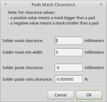
After opening your board in Pcbnew, make sure that your solder mask clearance and min width are set to zero. This is important because the manufacturers normally want to define the clearance themselves based on their process. Setting it to zero makes it easier for them to shrink/enlarge the pads for the solder mask. You find the dialogue under Dimensions > Pads to Mask Clearance:
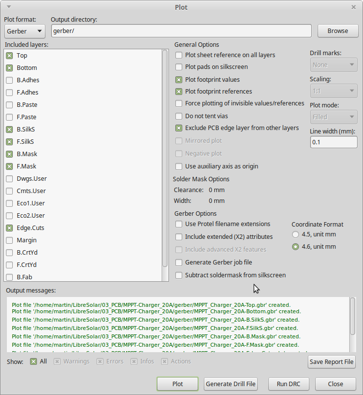
After that, open the Gerber export dialog under File > Plot and select at least the following layers for export:
- Top (Top copper plane)
- Bottom (Bottom copper plane)
- InX.Cu (Internal copper planes, if existing)
- B.Silk (Bottom silk screen: white plots with part names, etc.)
- F.Silk (Front silk screen)
- B.Mask (Bottom solder mask: inverted surface areas for the green paint of the PCB)
- F.Mask (Front solder mask)
- Edge.Cuts (Margins where the PCB should be cut by milling)
Select a folder where your files should be saved and press Plot:
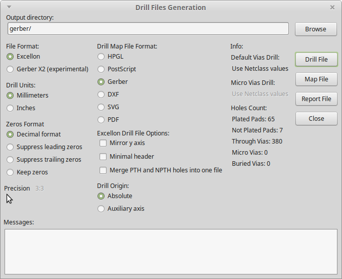
After sucessful export, press Generate Drill Files. Select the same output directory and make sure that Merge PTH and NPTH holes into one file is not checked. Otherwise, your manufacturer doesn’t know which holes are copper plated or not.
After that you should have all files necessary for the PCB production. Compress all files (gerber and drill files) to a .zip file and send them to the manufacturer.